- Fast turn-around within weeks – faster to market and significantly reduces development costs
Modular Photonics’ process is entirely mask-less. Designs created on a computer can be realised with the click of a button. This enables rapid iteration between design and testing to refine the circuit and the circuit’s performance. As a result, the customer is faster to market and it keeps the development costs low.
- Small volume prototyping to large volume production runs
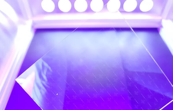
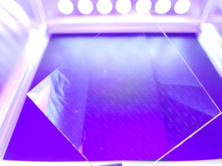
There is no capital expenditure for a mask and the throughput of the fabrication process results in low complexity circuits being fabricated within a few seconds. Yet, the process can be seamlessly scaled to fabricate entire glass wafers of photonic circuits.
- One-stop-shop: design, fabrication, testing and packaging
Modular Photonics is vertically integrated. It can rely on a team of specialists for designing, fabricating and testing of photonic circuits. Moreover, Modular Photonics has a proven platform for packaging photonic circuits and can pigtail the devices to single-mode, few-mode and multi-mode fibres and fibre arrays as well as polarization maintaining fibres.
- 3D photonic devices not possible with standard lithography
The 3-dimensional freedom of Modular Photonics’ process avoids waveguide crossovers. Unlike lithography, it also enables photonic circuits that simultaneously contain single-mode as well as multi-mode waveguides or circuits that feature waveguides which are specifically optimised for different wavelengths. It also facilitates the scalable fabrication of inherent 3D photonic devices, such as photonic lanterns.


